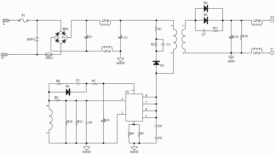
The influence of the RC value of the absorption circuit on VDS and VCS
2025/7/1 14:37:571.Schematic diagram
2. Analysis: The function of the absorption circuit in the figure is to absorb and release the energy stored in the leakage inductance of the transformer at the moment when the main power switch U1 is turned off.
According to the formula :P = 1/2* LK * I (t) ^2, LK=40uH
I (t) represents the charging current flowing through the absorption circuit of pair D3. As shown in Figure 1, the actual test maximum value is approximately 45V/100R =0.45A.
The time when the voltage is positive in Figure 1 is the charging time, which also corresponds to the time when the voltage of the absorption capacitor increases in Figure 4, approximately 320ns.
Assuming that the charging time of the capacitor is always at the maximum current, then P= 0.5* 0.000004* *0.45 *0.45 *0.00000032=0.000000405W. The power is very small and the discharge is very fast. The time for the voltage reduction of the absorbed capacitor in Figure 5 is approximately 520 ns. From the VDS waveform and the waveforms at both ends of the absorption capacitor, it can be seen that the total charging and discharging time for the peak formation is approximately 840ns, which is much shorter than the 14 us switching cycle. This means that the energy stored in the transformer leakage inductance can be discharged through the RCD in each cycle, and there is no phenomenon of energy accumulation and superposition.
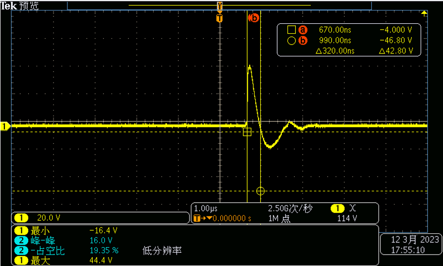
Figure 1 Voltage of R1
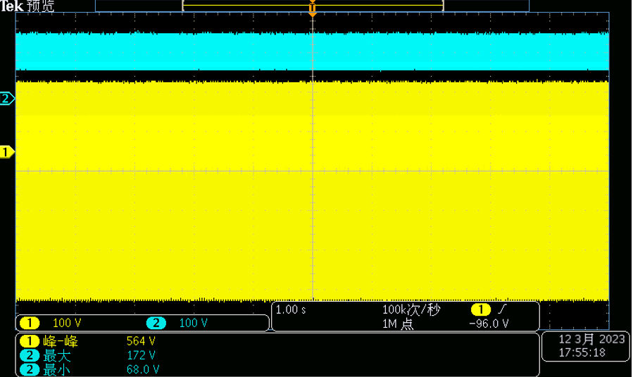
Figure 2 shows the voltage between pin D of the MOSFET and the positive terminal of VBuck. CH2 is the voltage across the absorption capacitor C3
Expand the waveform in Figure 2 to obtain the following waveform:
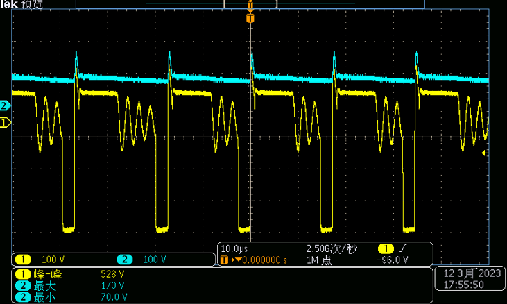
Figure 3
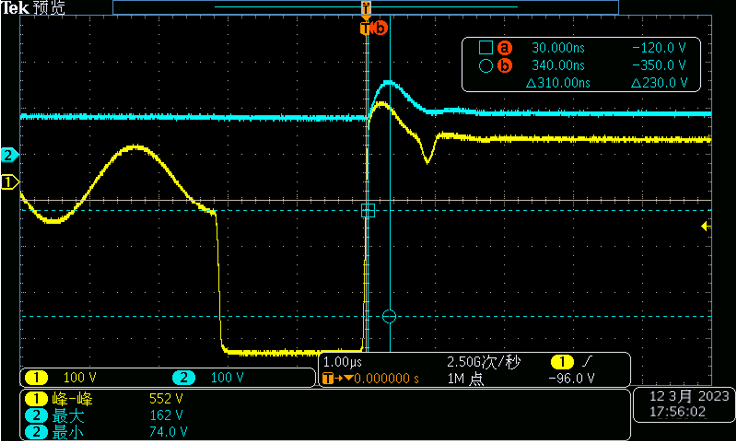
Figure 4
Technical Papers